(Hong Kong)

Product Summary
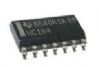
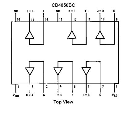
The CD4050BCN is a Hex Non-Inverting Buffer. It is monolithic complementary MOS (CMOS) integrated circuits constructed with N- and P-channel enhancement mode transistors. The CD4050BCN features logic level conversion using only one supply voltage (VDD). The input signal high level (VIH) can exceed the VDD supply voltage when the CD4050BCN is used for logic level conversions. It is intended for use as hex buffers, CMOS to DTL/ TTL converters, or as CMOS current drivers, and at VDD = 5.0V, it can drive directly two DTL/TTL loads over the full operating temperature range. The applications of the CD4050BCN include CMOS hex inverter/buffer, CMOS to DTL/TTL hex converter, CMOS current "sink" or "source" driver, CMOS HIGH-to-LOW logic level converter.
Parametrics
CD4050BCN absolute maximum ratings: (1)Supply Voltage (VDD): -0.5V to +18V; (2)Input Voltage (VIN): -0.5V to +18V; (3)Voltage at Any Output Pin (VOUT): -0.5V to VDD + 0.5V; (4)Storage Temperature Range (TS): -65℃ to +150℃; (5)Power Dissipation (PD) Dual-In-Line: 700mW; (6)Small Outline: 500mW; (7)Lead Temperature (TL) (Soldering, 10 seconds): 260℃.
Features
CD4050BCN features: (1)Wide supply voltage range: 3.0V to 15V; (2)Direct drive to 2 TTL loads at 5.0V over full temperature range; (3)High source and sink current capability; (4)Special input protection permits input voltages greater than VDD.
Diagrams
| Image | Part No | Mfg | Description |  |
Pricing (USD) |
Quantity | ||||
|---|---|---|---|---|---|---|---|---|---|---|
 |
 CD4050BCN |
|
IC BUFFER HEX NON-INV 16DIP |
Data Sheet |
Negotiable |
|
||||
 |
CD4050BCN_Q |
Fairchild Semiconductor |
Buffers & Line Drivers Hex Non-Inv Buffer |
Data Sheet |
Negotiable |
|
||||