(Hong Kong)

Product Summary
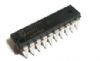
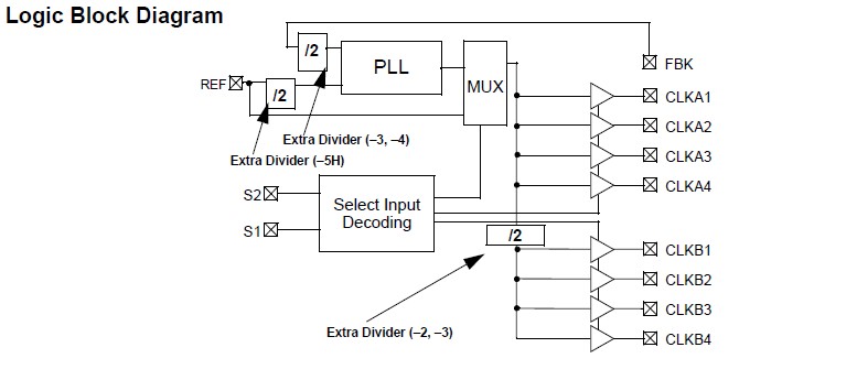
The CY2308SI-1 is a 3.3V Zero Delay Buffer designed to distribute high speed clocks in PC, workstation, datacom, telecom, and other high performance applications. The CY2308SI-1 has an on-chip PLL that locks to an input clock presented on the REF pin. The PLL feedback is driven into the FBK pin and obtained from one of the outputs. The input-to-output skew is less than 350ps and output-to-output skew is less than 200ps.
Parametrics
CY2308SI-1 absolute maximum ratings: (1)Supply Voltage to Ground Potential: –0.5V to +7.0V; (2)DC Input Voltage (Except Ref): –0.5V to VDD + 0.5V; (3)DC Input Voltage REF : –0.5 to 7V; (4)Storage Temperature: –65℃ to +150℃; (5)Junction Temperature: 150℃.
Features
CY2308SI-1 features: (1)Zero input-output propagation delay, adjustable by capacitive load on FBK input; (2)Multiple configurations; (3)Multiple low skew outputs; (4)Two banks of four outputs, three-stateable by two select inputs; (5)10 MHz to 133 MHz operating range; (6)75ps typical cycle-to-cycle jitter (15pF, 66 MHz); (7)Space saving 16-pin 150 mil SOIC package or 16-pin TSSOP; (8)3.3V operation; (9)Industrial Temperature available.
Diagrams
| Image | Part No | Mfg | Description |  |
Pricing (USD) |
Quantity | ||||
|---|---|---|---|---|---|---|---|---|---|---|
 |
 CY2308SI-1 |
|
IC CLK ZDB 8OUT 133MHZ 16SOIC |
Data Sheet |
Negotiable |
|
||||
 |
CY2308SI-1H |
Cypress Semiconductor |
Phase Locked Loops (PLL) 3.3VZDB COM |
Data Sheet |
Negotiable |
|
||||