(Hong Kong)

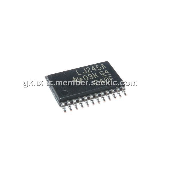
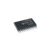
Product Summary
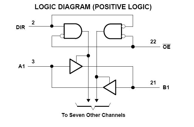
The LJ245A is an 8-bit octal bus transceiver and 3.3V to 5V shifter with 3-state outputs. It contains two separate supply rails; B port has VCCB, which is set at 3.3V, and A port has VCCA, which is set at 5V. This allows for translation from a 3.3V to a 5V environment, and vice versa. The LJ245A is designed for asynchronous communication between data buses. The LJ245A transmits data from the A bus to the B bus or from the B bus to the A bus, depending on the logic level at the direction-control (DIR) input. The output-enable (OE) input can be used to disable the device so the buses are effectively isolated. The control circuitry (DIR, OE) is powered by VCCA.
Parametrics
LJ245A absolute maximum ratings: (1)VCCA Supply voltage range –0.5 to 6.5V; (2)VI Input voltage range A port(2): –0.5V to VCCA + 0.5V; (3)Control inputs: –0.5V to 6V; (4)VO Output voltage range A port(2) –0.5 VCCA + 0.5 V; (5)IIK Input clamp current VI<0: –50mA; (6)IOK Output clamp current VO<0 :–50mA; (7)IO Continuous output current: ±50mA; (8)Continuous current through each VCCA or GND: ±100mA; (9)DB package: 63℃/W; (10)θJA Package thermal impedance(3) DW package 46℃/W; (11)PW package: 88℃/W; (12)Tstg Storage temperature range:–65 to 150℃.
Features
LJ245A features: (1)Bidirectional Voltage Translator; (2)5.5V on A Port and 2.7V to 3.6V on B Port; (3)Control Inputs VIH/VIL Levels Are Referenced to VCCA Voltage; (4)Latch-Up Performance Exceeds 250mA Per JESD 17; (5)ESD Protection Exceeds JESD 22; (6)2000V Human-Body Model (A114-A); (7)200V Machine Model (A115-A); (8)1000V Charged-Device Model (C101).
Diagrams